Optoelectronic device laboratory · Laboratory project
Organic Photovoltaics
Device fabrication and characterization
This laboratory project examines how fabrication conditions affect organic photovoltaic devices. It combines thin-film processing with optical absorption and current-density–voltage measurements.
Technologies: Organic photovoltaics, spin coating, electrode evaporation, absorption, J–V characterization
Device preparation
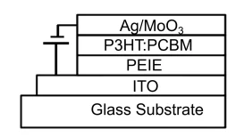
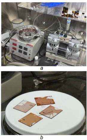
I prepared active and interfacial layers by spin coating and formed electrodes by evaporation. The sample set varies active-layer thickness and PEIE processing conditions.
Optical and electrical measurements
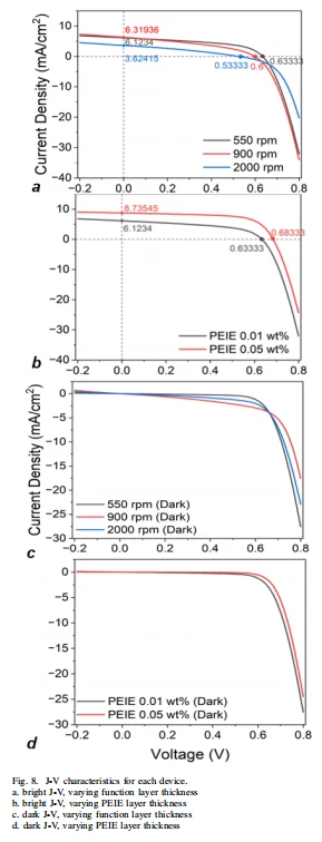
I compared optical absorption and J–V characteristics across the preparation conditions. The measured curves show how thickness and interfacial processing change the device response.